![[Compaq]](../../images/compaq.gif)
![[Go to the documentation home page]](../../images/buttons/bn_site_home.gif)
![[How to order documentation]](../../images/buttons/bn_order_docs.gif)
![[Help on this site]](../../images/buttons/bn_site_help.gif)
![[How to contact us]](../../images/buttons/bn_comments.gif)
![[OpenVMS documentation]](../../images/ovmsdoc_sec_head.gif)
| Document revision date: 19 July 1999 | |
|
|
|
|
|
|
| Previous | Contents | Index |
Return from Exception or Interrupt
opcode
| N|| <--- saved PSL<3>; | |
| Z|| <--- saved PSL<2>; | |
| V|| <--- saved PSL<1>; | |
| C|| <--- saved PSL<0>; |
| 02 | REI | Return from Exception or Interrupt |
A longword is popped from the current stack and held in a temporary program counter (PC). A second longword is popped from the current stack and held in a temporary processor status longword (PSL).The popped PSL is checked for internal consistency. If the processor is running virtual machine (VM) mode, the popped PSL is compared with the Virtual-Machine Processor Status Longword (VMPSL) to determine that the transition from current VMPSL to popped PSL is allowed, and a VM-emulation trap is taken. If the processor is running a real machine, the popped PSL is compared with the current PSL to determine that the transition from current PSL to popped PSL is allowed.
If the processor is not in kernel mode and is attempting to return to a PSL with the VMPSL VM bit set, a reserved operand fault occurs. The current stack pointer (SP) is saved, and a new SP is selected according to the new PSL CUR_MOD and IS fields. The level of the highest privilege asynchronous system trap (AST) is checked against the current mode to see whether a pending AST can be delivered. Execution resumes with the instruction being executed at the time of the exception or interrupt.
After completing an REI, a processor will correctly execute a modified instruction stream.
Load Process Context
opcode
| N|| <--- N; | |
| Z|| <--- Z; | |
| V|| <--- V; | |
| C|| <--- C; |
| 06 | LDPCTX | Load Process Context |
If the processor is in virtual machine (VM) mode, and the virtual machine is in kernel mode, then a VM-emulation trap is taken. Otherwise, if the processor is not in kernel mode, a privileged-instruction fault is taken. If neither exception is taken, the processor loads the process state in the process control block (PCB) specified by the privileged process control block base register (PCBB).The general registers, process-space memory management registers, and the address space number register (if implemented) are loaded from the PCB into the scalar processor. Execution is switched to the kernel stack. The program counter (PC) and processor status longword (PSL) are moved from the PCB to the stack, suitable for use by a subsequent REI instruction.
If the processor implements an address space number (ASN) register, the process translation buffer (TB) state associated with the new value of the ASN (that is, the one loaded by the LDPCTX instruction) is flushed if the process last ran on a different processor. This is indicated by the previous CPU (PRVCPU) field being not equal to the CPU identification (CPUID) register. If the processor does not implement the ASN register, the process-space TB state is unconditionally flushed.
Save Process Context
opcode
| N|| <--- N; | |
| Z|| <--- Z; | |
| V|| <--- V; | |
| C|| <--- C; |
| 07 | SVPCTX | Save Process Context |
If the processor is in virtual machine (VM) mode, and the virtual machine is in kernel mode, then a VM-emulation trap is taken. Otherwise, the process control block (PCB) is specified by the privileged process control block base register (PCBB). The general registers are saved into the PCB. The program counter (PC) and processor status longword (PSL) currently on the top of the current stack are popped and stored in the PCB. If the processor implements the adress space number (ASN) register, then the CPU identification (CPUID) register is saved in the previous CPU (PRVCPU) field in the PCB. If a SVPCTX instruction is executed when the interrupt stack (IS) is clear, then IS is set, the interrupt stack pointer (ISP) is activated, and interrupt priority level (IPL) is maximized with 1 because of the switch to the IS.
Move to Processor Register
opcode src.rl, procreg.rl
| N|| <--- UNPREDICTABLE | |
| Z|| <--- UNPREDICTABLE | |
| V|| <--- UNPREDICTABLE | |
| C|| <--- UNPREDICTABLE |
| DA | MTPR | Move to Processor Register |
If the processor is in virtual machine (VM) mode, and the virtual machine is in kernel mode, then a VM-emulation trap is taken. MTPR loads the source operand specified by src into all copies of the processor register specified by procreg that are implemented on the vector and scalar processors. The procreg operand is a longword that contains the processor register number. Execution may have register-specific side effects.
Move from Processor Register
opcode procreg.rl, dst.wl
| N|| <--- UNPREDICTABLE | |
| Z|| <--- UNPREDICTABLE | |
| V|| <--- UNPREDICTABLE | |
| C|| <--- UNPREDICTABLE |
| DB | MFPR | Move from Processor Register |
If the processor is in virtual machine (VM) mode, and the virtual machine is in kernel mode, then a VM-emulation trap is taken. The destination operand is replaced by the contents of the processor register specified by procreg. The procreg operand is a longword that contains the processor register number. Execution may have register-specific side effects.
Bugcheck
opcode message.bx
| N|| <--- N; | |
| Z|| <--- Z; | |
| V|| <--- V; | |
| C|| <--- C; |
| FEFF | BUGW | Bugcheck with word message identifier |
| FDFF | BUGL | Bugcheck with longword message identifier |
The hardware treats these opcodes as reserved to Digital and as faults. The OpenVMS operating system treats them as requests to report software detected errors. The inline message identifier is zero extended to a longword (BUGW) and interpreted as a condition value (see the VAX Procedure Calling and Condition Handling Standard in the OpenVMS Programming Interfaces: Calling a System Routine). If the process is privileged to report bugs, a log entry is made. If the process is not privileged, a reserved instruction is signaled.
| #1 |
|---|
BUGW                   ; Bugcheck with word message
.WORD    4             ;   identifier 4

BUGL                   ; Bugcheck with longword
.LONG    5             ;   message identifier 5
|
This chapter describes an extension to the VAX architecture for
integrated vector processing. Some VAX vector architecture departs from
the traditional VAX scalar architecture, especially in the areas of
UNPREDICTABLE results, vector processor exceptions, and
instruction/memory synchronization.
10.1 Introduction to VAX Vector Architecture
Implementation of the VAX vector architecture is optional. VAX processors that do implement the vector architecture do so as specified in this chapter. Operating system software may emulate the vector architecture on processors that omit this feature.
On VAX processors that omit the vector architecture, vector instructions result in a reserved-instruction fault.
The vector architecture features include additional instructions, vector registers, and vector control registers.
All descriptions and examples of vector instructions in this chapter
use the assembler notation form of instructions, as described in
Section 10.5. The number and order of operands for the assembler
notation differ from that defined in the instruction stream format. See
Section 10.3 and Section 10.5 for additional information.
10.2 VAX Vector Architecture Registers
This section identifies and describes the vector, vector control, and
internal processor registers used in processing vector architecture
operations.
10.2.1 Vector Registers
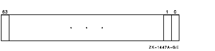
There are 16 vector registers, V0 to V15. Each vector register contains 64 elements numbered 0 to 63. Each element is 64 bits wide. Figure 10-1 depicts a vector register.
Figure 10-1 Vector Register

A vector instruction that performs a register-to-register operation is defined as a vector operate instruction. A vector operate instruction that reads or writes F_floating data, or integer data for shifts or integer arithmetic operations, reads bits <31:0> of each source element and writes bits <31:0> of each destination element. Bits <63:32> of the destination are UNPREDICTABLE for F_floating, integer arithmetic, and shift instructions.
Vector logical instructions read bits <31:0> of each source element and write the result into bits <31:0> of each destination element; bits <63:32> of the destination element receive bits <63:32> of the corresponding element of the Vb source operand.
For vector instructions that read longword data from memory into a vector register (VLDL and VGATHL), bits <63:32> of the destination elements are UNPREDICTABLE.
If the same vector register is used as both source and destination in a Gather Memory Data into Vector Register (VGATH) instruction, the result of the VGATH instruction is UNPREDICTABLE.
For the IOTA vector instruction, bits <63:32> of the destination
elements are UNPREDICTABLE.
10.2.2 Vector Control Registers
The 7-bit Vector Length Register (VLR), shown in Figure 10-2, limits the highest vector element to be processed by a vector instruction. VLR is loaded prior to executing the vector instruction using a Move to Vector Processor (MTVP) instruction. The value in VLR may range from 0 to 64. If the vector length is zero, no vector elements are processed. If a vector instruction is executed with a vector length greater than 64, the results are UNPREDICTABLE. Elements beyond the vector length in the destination vector register are not modified.
Figure 10-2 Vector Length Register (VLR)

The Vector Mask Register (VMR), shown in Figure 10-3, has 64 bits, each corresponding to an element of a vector register. Bit <0> corresponds to vector element 0. See Section 10.3.1 for information on masked operations.
Figure 10-3 Vector Mask Register (VMR)
The 7-bit Vector Count Register (VCR), shown in Figure 10-4, receives the length of the offset vector generated by the IOTA instruction.
Figure 10-4 Vector Count Register (VCR)

These registers are read and written by Move from/to Vector Processor
(MFVP/MTVP) instructions.
10.2.3 Internal Processor Registers
The vector processor contains the following internal processor registers (IPRs) that can be accessed by the scalar processor using MTPR/MFPR instructions:
The VPSR is shown in Figure 10-5, and is described in Table 10-1.
Figure 10-5 Vector Processor Status Register (VPSR)

| Extent | Type | Description |
|---|---|---|
| <0> | R/W | Vector Processor Enabled (VEN). The vector processor is enabled by writing a one to this bit. Writing a zero disables the vector processor. If VPSR<VEN> is cleared by software while VPSR<BSY> is set, then once the new state of VPSR becomes synchronized with subsequent vector instructions, no more instructions are sent and the vector processor completes execution of all pending instructions in its instruction queue. See Section 10.6.3, Vector Processor Disabled, for more details. |
| <1> | W | Vector Processor State Reset (RST). Writing a one to this bit clears VPSR and VAER. If VPSR<RST> is set by software while VPSR<BSY> is set, the operation of the vector processor is UNDEFINED. This bit is read as zero (RAZ). |
| <2> | W | Vector State Store (STS). Writing a one to this bit initiates storing of implementation-specific vector state information to memory using the address in VSAR for the asynchronous method of handling memory management exceptions. If the synchronous method is implemented, write operations to VPSR<STS> are ignored. This bit is RAZ. |
| <3> | W | Vector State Reload (RLD). Writing a one to this bit initiates reloading of implementation-specific vector state information from memory using the address in VSAR for the asynchronous method of handling memory management exceptions. If the synchronous method is implemented, write operations to VPSR<RLD> are ignored. This bit is RAZ. |
| <4> | R | 0 |
| <5> | R/W1C | Memory Fault (MF). This bit is set by the vector processor when there is a memory reference to be retried due to an asynchronous memory management exception. Writing a one to VPSR<MF> clears it. Writing a zero to VPSR<MF> has no effect. If the synchronous method of handling memory management exceptions is implemented, this bit is always zero. |
| <6> | R/W1C | Pending Memory Fault (PMF). This bit is set by the vector processor when an asynchronous memory management exception is pending. Writing a one to VPSR<PMF> clears it. Writing a zero to VPSR<PMF> has no effect. If the synchronous method of handling memory management exceptions is implemented, this bit is always zero. |
| <7> | R/W1C | Vector Arithmetic Exception (AEX). This bit is set by the vector processor when disabling itself due to an arithmetic exception. Information regarding the nature of the exception can be found in VAER. Writing a one to VPSR<AEX> clears VPSR<AEX> and VAER. Writing a zero to VPSR<AEX> has no effect. |
| <23:8> | R | 0 |
| <24> | R/W1C |
Implementation-Specific Hardware Error (IMP). This bit is set by the
vector processor when disabling itself due to an
implementation-specific hardware error. Writing a one to
VPSR<IMP> clears it. Writing a zero to VPSR<IMP> has no
effect.
An implementation may choose not to implement VPSR<IMP>. In this case, writing VPSR<IMP> with either value must have no effect and must not generate any error. Also, its value when read must be zero. |
| <25> | R/W1C |
Illegal Vector Opcode (IVO). This bit is set by the vector processor
when disabling itself due to receiving an illegal vector opcode.
Writing a one to VPSR<IVO> clears it. Writing a zero to
VPSR<IVO> has no effect.
An implementation may choose not to implement VPSR<IVO>. In this case, writing VPSR<IVO> with either value must have no effect and must not generate any error. Also, its value when read must be zero. |
| <30:26> | R | 0 |
| <31> | R | Vector Processor Busy (BSY). When this bit is set, the vector processor is executing vector instructions. When it is clear, the vector processor is idle, or the vector processor has suspended instruction execution due to an asynchronous memory management exception or hardware error. Writing to VPSR<BSY> has no effect. |
Table 10-2 shows the possible settings of VPSR<3:0> in the same MTPR instruction, and the resulting action for the vector processor. The state of the vector processor is determined by the encoding of Vector Processor Enabled (VPSR<VEN>) and Vector Processor Busy (VPSR<BSY>). The vector processor state for possible encodings is shown in Table 10-3.
| RLD | STS | RST | VEN | Meaning |
|---|---|---|---|---|
| 0 | 0 | 0 | 0 | Disable vector processor |
| 0 | 0 | 0 | 1 | Enable vector processor |
| 0 | 0 | 1 | 0 | Reset state and disable vector processor |
| 0 | 0 | 1 | 1 | Reset state and enable vector processor |
| 0 | 1 | 0 | 0 | Store state (must disable vector processor) |
| 1 | 0 | 0 | 0 | Reload state and disable vector processor |
| 1 | 0 | 0 | 1 | Reload state and then enable vector processor |
| VEN | BSY | Meaning |
|---|---|---|
| 0 | 0 | The vector processor is not executing any instructions now, and either has no pending instructions or will not execute pending instructions. No more instructions should be sent. |
| 0 | 1 | The vector processor is executing at least one pending instruction. No more instructions should be sent. |
| 1 | 0 | The vector processor is not executing any instructions now, and either has no pending instructions or will not execute pending instructions. New instructions can be sent to the vector processor. |
| 1 | 1 | The vector processor is executing at least one instruction now. New instructions can be sent. |
| Previous | Next | Contents | Index |
|
|
| privacy and legal statement | ||
| 4515PRO_030.HTML | ||